Silicon and oxygen are most abundant elements on earth, most of it is combined to make silica, the material of which most sand and rocks are made. Most sand is brownish in color because it contains a large amount of impurities. Only the purest sand is selected to be used in the manufacture of semiconductor chips.
The sand must have the oxygen removed from it to create pure silicon. To do this the sand is mixed with carbon and the mixture is heated to over 2,000oC. This causes the oxygen in the sand to react with the carbon, producing carbon dioxide, and near pure silicon.
But the silicon is still not pure enough for the manufacture of semiconductor chips. The silicon is next ground to a fine powder and treated with gaseous hydrogen chloride at a temperature up to 1,000oC. The result is amorphous silicon, it must be transformed into crystalline silicon.
The amorphous silicon is placed in a rotating crucible and heated to a temperature above 1,140oC until it melts. A tiny crystal of silicon is then dipped into the molten silicon while it's still rotating. As the tiny crystal is slowly lifted out of the crucible, it acts as a seed, causing silicon from the crucible to crystallize around it.
![]()
Silicon Wafer [Picture from Wikimedia Commons]
As the crystal is slowly pulled up from the rotating crucible, the silicon builds up as a rod, typically 300mm in diameter. The crystal rod is ground to uniform diameter and a diamond saw is used to cut it into circular wafers, typically 0.775mm thick. The surfaces of the wafers are then polished flat to within 2µm (2 micrometer, 0.002 mm, or about 0.000078 inch), giving them a mirror-like luster.
To create electronic circuits on a wafer, it's heated in a furnace and exposed to pure oxygen which forms a silicon dioxide film of uniform thickness across the surface of the wafer. A layer of photoresistive film is applied to the surface of the wafer, giving it characteristics similar to photographic paper.
The wafer is then exposed to intense light through a mask. The mask defines the pattern of circuit features by protecting the areas where photoresist is to not be removed. The mask is much larger than the actual electronic circuits will be, so the pattern is projected through a reducing lens.
A developer solution is used to etch away the photoresist where the mask did not protect it from exposure to the light. A gaseous stream of dopant element atoms is directed at the exposed areas of the wafer causing the dopant atoms to embed themselves into the silicon. This creates the n-type and p-type regions.
The masking, exposing, etching, and doping steps are repeated several times to create the different circuit layers of the chip. The individual circuits are interconnected using a series of metal depositions and dielectric film insulation depositions.

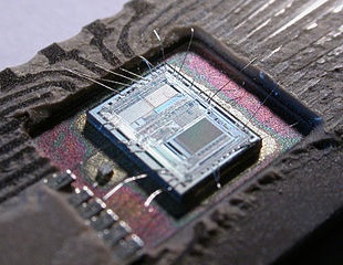
Chip Package [Picture from Wikimedia Commons]
After the last last layer of metal connection pattern is deposited, a final insulating layer of dielectric is deposited to protect the circuit. Openings are etched into this insulating film to allow the connection of contact leads.
Each wafer has hundreds of chips, a diamond saw is used to cut the wafer into individual chips. The chips are then assembled into a package that provides contact leads for the chip.
More Computer Architecture Articles:
• Microcontroller Registers
• Operating System Processes
• ARM Cortex-A72 Registers
• Intel Celeron D Processor
• Challenges of Programming Multicore Systems
• The Evolution of Hard Disk Bit Recording
• The Fetch, Decode, Execute Cycle
• AMD Sempron Processor
• Factors in Choosing an Oscilloscope
• Using The I2C Bus

