The Fetch, Decode, Execute cycle is paramount to the functioning of a microprocessor. In this article I'll describe the Fetch, Decode, Execute cycle simplified to its bare-bones in a highly simplified fictitious microprocessor.
The Program Counter (PC) is a microprocessor register that simply counts. If the microprocessor where executing a program that does nothing, the Program Counter would sequentially step through memory addresses. However most programs don't sequentially step through memory addresses, they loop and branch. Therefore the actual address of the location in memory to be accessed is found in another register called the Memory Address Register (MAR). The address in the MAR may come from the PC or from the Instruction Decoder (ID).
Lets design a very simple program to see how the Fetch, Decode, Execute cycle works.
1. ADD 5,6
2. STOR 3
3. 0
Fetch

The first thing the program does is fetch the instruction located at memory address 1. To do this the MAR performs a memory read operation, causing the contents of memory address 1 to be transferred over data bus to the ID.
Decode
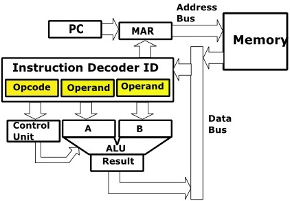
The ID decodes the contents of memory address 1, determining that it is an ADD instruction, and it's the type of ADD instruction that contains the values to be added in the second and third parts of the instruction.
Execute
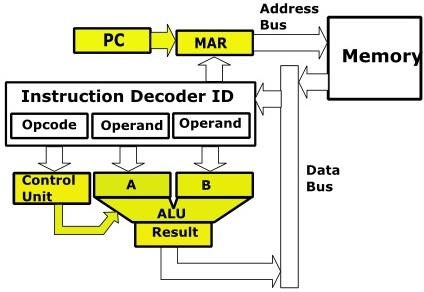
The ID, now knowing exactly what to do with the instruction it has received transfers the values to be added to the input registers of the Arithmetic Logic Unit (ALU) and activates control lines that cause the ALU to add the two values and place the results in its output register. That instruction having been completed the PC increments to the next value and places the value in the MAR.
Fetch
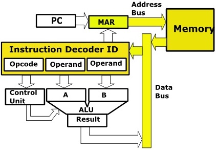
This causes the instruction located at memory address 2 to be to be transferred over data bus to the ID.
Decode
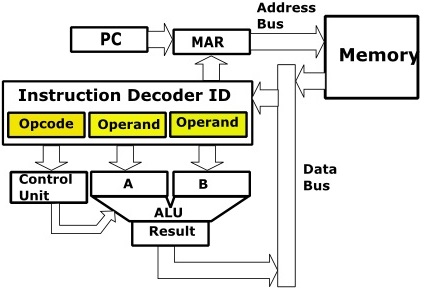
The ID decodes the contents of memory address 2, determining that it is a STOR instruction, and it's the type of STOR instruction that indicates the that the contents of the ALU output register should be stored at the memory address contained in the second part of the instruction.
Execute
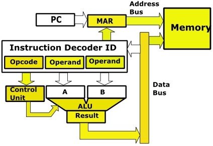
The ID, now knowing exactly what to do with the instruction it has received activates control lines that cause the contents of the ALU output register to be placed on the data bus, the memory address in the instruction to be placed in the MAR, and the MAR instructed to perform a write operation.
Shown below is the state of memory after the above two Fetch, Decode, Execute cycles.
1. ADD 5,6
2. STOR 3
3. 11
Of course we know that most programs contain thousands or millions of instructions, and therefore the Fetch, Decode, Execute would be performed repeatedly until the last instruction causes the program to exit.
This is agreeably a very simple description of the Fetch, Decode, Execute cycle performed in a microprocessor, but we can build on this to get a better understanding of how more complex instructions work and how an instruction pipeline works.
More Computer Architecture Articles:
• Digital Logic Semiconductor Families
• The Microcontroller Memory Map
• Fundamental Digital Logic Gates
• Interrupt Request Lines (IRQs)
• Learn Assembly Language Programming on Raspberry Pi 400
• Dynamic Loading of Program Routines and Dynamically linked libraries (DLLs)
• Getting started with Raspberry Pi
• Computer Buses
• Introduction to the Raspberry Pi
• Basic Computer Architecture

