Over the development time of the computer, several different designs of packaging for the CPU chip die have been used. Each type of packaging has its advantages and disadvantages. Today's most advanced CPUs come in the LGA (Land Grid Array) package, but lets review some common packages that might still be in use.
DIP

A DIP chip package has two parallel rows of pins (Dual In-line Pins). This package was developed in the 1960s because no transistor package could handle the number of connections required by integrated circuits. The package's pins were inserted into through-holes on a printed circuit board and then soldered. This was a good package for prototyping because the pins could also be inserted into a socket.
PGA

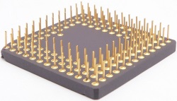
When processor with larger width data buses were developed, the DIP package could not handle the number of connections required. The PGA (Pin Grid Array) aleviated this problem by allowing pins to be arranged in an array on the underside of the package.

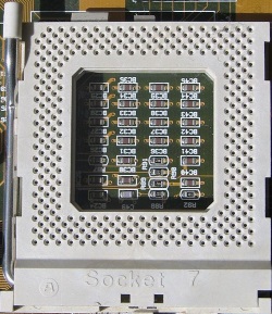
PGAs pins were sometimes inserted into through-holes on a printed circuit board and then soldered, but it was common to mount CPU PGA's into special ZIF (Zero Insertion Force) sockets so that when more powerful CPU's were released, the chip could be upgraded.
A "flip-chip" PGA has the die mounted on the top of the substrate to allow a heatsink to be placed in closer contact with the die. The substrate was frequently made of ceramic to allow better conduction of heat from the die.
BGA

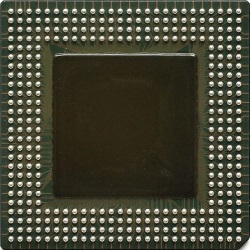
The BGA (Ball Grid Array) was designed to lower the cost of CPU and computer motherboard manufacturing, and at the same time improve reliability. With a BGA package, the pins are eliminated, replaced by tiny copper pads, each with a tiny ball of solder held to it with tacky flux. The BGA is accurately held in place while the printed circuit board is heated, forming soldered connections between the CPU and the circuit board.
Elimination of the pins saves the cost of the pins, plus pin connections are less reliable than directly soldered connections.
LGA

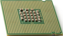
Because the soldering of BGA devices requires precise control, it can only be accomplished using automated processes. further more, BGA devices are not suitable for socket mounting. However, one of the most common practices with computers is to upgrade the CPU. The LGA (Land Grid Array) has a grid of copper contacts on the underside of a package. This allows the package to be used with a socket or be soldered down using surface mount technology.
When used with a socket, the pins are on the socket rather than on the LGA package. When soldered directly to the circuit board, solder paste is applied to the copper contacts on the LGA package.
More Computer Architecture Articles:
• Operating System Processes
• The Computer's Chipset
• The Microcontroller's Asynchronous Serial Interface
• Pi-Top kit - Build Your Own Laptop
• Data Structures - Linked List, Stack, Queue, and Tree
• How Computer Memory Works
• Digital Logic Transfer Characteristics
• The Fetch, Decode, Execute Cycle
• The Use of SOI (Silicone on Insulator) Wafers in MEMS (Micro-Electro-Mechanical Systems) Production
• Basic Arithmetic Logic Unit (ALU) Circuitry

