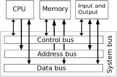
An important part of Von Neumann's stored program architecture is the memory, because that is where not only the program is stored, but also where the data that the program works on, and any temporary results are stored. Although a computer uses all kinds of memory for various functions, the memory where the program can be executed and the data is manipulated is called "main memory".
Every program being executed and every piece of data being manipulated must be copied from a storage device, such as a magnetic disk, into main memory. The amount and speed of main memory is possibly the most important factor in determining the power of a computer.
Types of Memory
It's important to understand the basic types of memory. When computer data is "backed up" it is usually backed up to a tape drive. A tape drive represents "serial" or "sequential" memory. With serial memory, data is accessed sequentially. This has the disadvantage that access time depends on the location of the desired data on the serial storage device.
Random Access Memory (RAM) is a type of memory where any byte of memory can be accessed randomly, without examining the preceding bytes. The term RAM is also used to distinguish read⁄write memory from Read Only Memory (ROM) which is unfortunate because ROM is also accessed randomly.
Whereas you can read and write data to RAM any number of times, you can write to ROM only one time. After that you can only read from the ROM memory. The term ROM is also used to distinguish non-volatile memory from volatile memory. With volatile memory, when the computer power is lost, so is the data in the RAM.
However, with ROM, data is not lost when the computer power is lost. ROM is important because it contains the basic programming and data that allows your computer to be "booted up" or restarted each time you turn it on.
If you're not confused enough about the different types of memory, there are also various types of "electrically alterable" ROM memory. These devices normally work like a ROM, that is read only, but with the proper control signals they can be re-written. Most of the time these are referred to as EPROM (Erasable Programmable ROM), but they can also be called EAROM, EEPROM, E^2PROM, and may other contractions.
RAM can also be divided into "static" and "dynamic" types. You might think dynamic RAM (DRAM) must be far superior to static RAM (SRAM), but no. DRAM is used for the computers main memory because it's cheap to manufacture. However, like everything in life, there are always trade-offs. The trade-off with DRAM is that it quickly loses its contents. It must be constantly "refreshed", and this requires complicated circuitry.
How a Capacitor Works
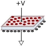
A capacitor consists of two conductor plates which are very close to each other, but have a dielectric insulator between them. When you apply an electric charge across a capacitor, electrons can't flow through the insulator, so they build up on the plate connected to the negative voltage source. Although electrons can't flow through the insulator, an electrostatic charge can pass through the insulator, thus repelling electrons on the opposite plate, causing it to gain a positive charge.
If you apply a positive electric voltage to a capacitor, and then remove its continuity to the circuit, it will retain the voltage. Obviously, if the voltage is equal to the level defined as binary 1, you have stored a binary bit. If you restore the continuity with zero volts, the capacitor will discharge. If you then remove its continuity, you have stored a binary 0. This is how a binary bit is stored in DRAM.
CMOS Dynamic Memory Cell
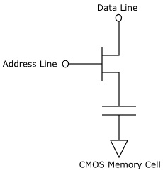
To write a binary bit to the cell, select it by applying a voltage to the Address line. This causes the transistors channel to conduct, making the voltage on the capacitor appear on the Data Line.
To write a binary 1 to the cell, apply a voltage to the Data Line. This charges the capacitor. To write a binary 0 to the cell, apply 0 volts to the Data Line. This discharges the Data Line. If you write a binary 1, the capacitor has a tiny leakage which will cause the charge to be lost, therefore it is necessary to rewrite the data periodically. This is called "refreshing".
To read a cell, select it by applying a voltage to the Address line. This causes the transistor's channel to conduct, making the voltage on the capacitor appear on the Data Line. The read operation discharges the capacitor, so a write operation to restore the voltage should follow the read.
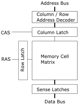
On a DRAM chip the cells are laid out in a matrix of columns and rows. To read data from the DRAM the CPU memory controller activates the RAS (Row Access Strobe) line to select the memory address and then it activates the CAS (Column Access Strobe) line to access the data at that memory address.
The data is transferred to a row of sense amplifiers and then to latches to temporarily hold the data. During a read operation, after reading, the latches rewrite the data to the accessed address. But normal memory accesses can't be relied upon to refresh the DRAM within the necessary time, which is in the millisecond range. So a separate refresh process refreshes each memory cell within the maximum interval specified by the DRAM manufacturer.
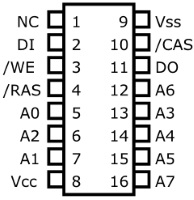
Shown above is the pinout for the 2164 DRAM chip. This is a 64K x 1 bit memory chip, so you would need x number of chips depending upon the word size of your CPU. To read a memory location, the /WE (Write Enable) must be inactive (high), the address must be applied to the A0 - A7 pins, then when the /RAS and /CAS pins are active (low), the data will be available at the DOUT pin.
To write a memory location, the /WE (Write Enable) must be active (low), the address must be applied to the A0 - A7 pins, then the /RAS and /CAS pins must be active (low), and the data placed on the DIN pin. Then the /WE, /RAS, and /CAS must be made inactive (high). For the refresh-only cycle, the /CAS pin is held inactive (high). Only the /RAS is strobed active (low).

There are 8 chips on this RAM stick to store an 8-bit byte. No, you're not counting wrong. This chip actually has 9 chips. The extra chip is used to hold a "parity" bit. Used to verify the integrity of the data stored in RAM. In the "even" parity system, if the total number of ones in a byte is an odd number, the parity bit is set to one, thus making an even number of ones. When the data is read back, the system checks the parity of the byte with parity bit to make sure it hasn't been corrupted. There is also an odd parity scheme.
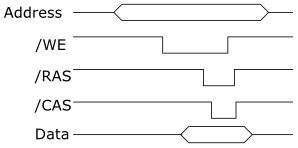
The above waveform diagram shows a DRAM memory write. The address appears on the address lines and is latched when /WE goes low. Then the data is placed on the data line. Next /RAS goes low. Then /CAS goes low, which latches the data into the memory location. Finally /RAS, /CAS, and /WE are returned to their inactive state (high).
SDRAM (Synchronous DRAM)
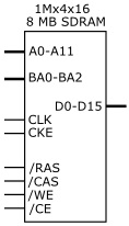
Whereas DRAM operates asynchronously (it responds based on control signals), SDRAM adds a clock input, which allows it to be synchronized with the system clock. This allows it to operate at higher speed, and allows it to support "burst" mode so that it can transfer an entire block of data.
SDRAM control signals
| CLK | Clock signal. |
| CKE | Clock Enable. When low ignores clock. |
| /CS | Chip Select. When high ignores all other inputs. |
| /RAS | Row Address Strobe. |
| /CAS | Column Address Strobe. |
| /WE | Write enable. When low, along with /RAS and /CAS, allows memory write. |
| BAn | Bank Selection. Internally SDRAMs are divided into2, 4 or 8 independent banks. BA0, BA1 and BA2 are used to select a bank. |
DDR SDRAM (Double Data Rate SDRAM)
DDR SDRAM operates at higher speed by transferring data on both the rising and falling edges of the clock signal (known as "double pumping"). Whereas typical speeds of SDRAM are 100 and 166 MHz, DDR clock speeds range between 200 MHz (DDR-200) and 400 MHz (DDR-400).
| Device | Voltage | Bus clock | Transfer rate |
| SDRAM | 3.3 | 100-166 | 0.8-1.3 GB/s |
| DDR | 2.5-2.6 | 133-200 | 2.1-3.2 GB/s |
| DDR2 | 1.8 | 266-400 | 4.2-6.4 GB/s |
| DDR3 | 1.35-1.5 | 533-800 | 8.5-14.9 GB/s |
| DDR4 | 1.2 | 1066-1600 | 17-21.3 GB/s |
DDR2 SDRAM is twice as fast as DDR. Clock speeds range between 400 MHz (DDR2-400) and 800 MHz (DDR2-800). DDR3 is twice as fast as DDR2. Clock speeds range between 800 MHz (DDR3-800) and 1600 MHz (DDR3-1600). DDR4 is twice as fast as DDR3 and operates at a frequency between 1600 and 3200 MHz.
More Computer Architecture Articles:
• Monolithic Kernel vs Microkernel vs Hybrid Kernel
• Binary Number Representation and Binary Math
• Operating System Memory Allocation Methods
• First-Come, First-Served CPU Scheduling Algorithm
• Operating System Processes
• Intel's Dual-Core Core i3 Processor
• The Microcontroller Memory Map
• Load Balancing Multiple CPUs in Symmetric Multiprocessing
• Operating System Memory Management
• Operating System Memory Paging

